Introduction
A leading UK semiconductor device research group at the University of Glasgow approached us with a requirement for an RF magnetron sputtering tool. It was to have the capability of producing an all-thin-film interference device to give a specific reflectivity on the surface of GaAs wafers used to fabricate laser diodes. The requirement specification was arrived at by modelling a notional thin film stack reflectivity performance on the surface of a crystalline wafer. This technique is very often used in the world of glass optics to achieve modifications which can manipulate the optical transmission and reflection of surfaces.
The Reflector Design
Using a proprietary modeling package we could determine the stack design needed to produce the reflectivity specification. That specification was to be a minimum of 60% reflectivity at normal incidence and at 765 nm on crystalline GaAs. Selection of a silicon target with the capability to switch between a gas inlet of oxygen or nitrogen (or a mixture), as well as argon for the plasma, would give the capability to produce silicon oxides, silicon nitrides and mixed oxy-nitrides. SiO2 has a visible/NIR refractive index of around 1.45 and Si3N5 has an index close to 2. These numbers are ideal for a simple stacked reflector like this:
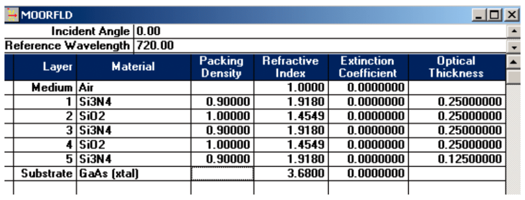
And theoretically this stack gives a reflectivity like this:
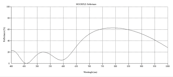
This became our starting point….
Practical Fabrication
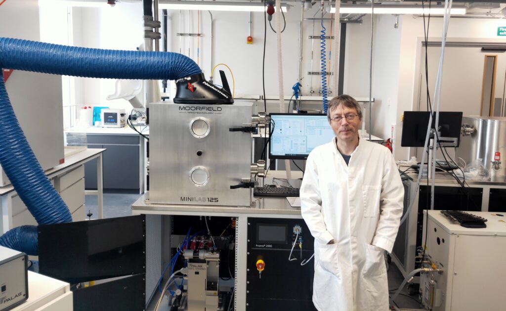
The first thing that the practical fabrication of all such structures requires is the deposition of single layers of material with physical and optical characteristics that will enable us to build the device. That means we need homogenous, continuous thin films of the individual materials which adhere to a substrate, won’t peel or rub off and, for optical devices like this, will have substantially the correct refractive index and are free from optical absorption. To this end, we specified and built a system based on the MiniLab 125 platform. With the machine built and operational, we moved on rapidly with deposition experiments…
In fact, RF sputtering on its own is not entirely suitable for dielectrics like this. Their deposition rate is slow, crystalline micro-structure can be poor and without careful design of the deposition chamber, target contamination can be a showstopper. However, Moorfield has many years’ experience in this kind of work, so we weren’t exactly starting from scratch.
Very quickly it became apparent that ambient substrate temperatures, although leading to physically well-structured films, would always give us optical absorption. Some substrate heating dealt with that problem and once the quartz test pieces were heated to 200 °C, optical absorption disappeared as a result of improved micro-crystalline structure and compositions close to stoichiometry. Quartz test pieces? GaAs isn’t transparent at 765 nm, so there is no choice other than to deposit initially onto something else.
With a set of deposition parameters ready to give us transparent films, we then needed to calibrate for tooling factor – the relationship between deposition parameters and the deposited thickness on the substrate. Keeping all deposition parameters constant, the tooling factor is simply related to the deposition time – the longer the shutter is open, the more material is deposited. By measuring the thickness of a film and relating it to its deposition time, we can easily calculate the times required to deposit the thicknesses needed in the stack.
The one problem in this simple route forward is that we have single layers and test structures on quartz. We wanted the final result on GaAs, of course…
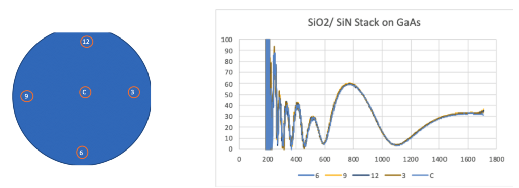
That’s a relatively simple thing to modify in the modeling software and when we look at the performance on quartz and the performance on GaAs, we can infer the changes needed to hit the required spec on GaAs. Here’s the final result:
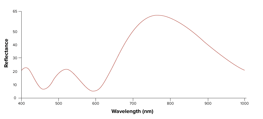
The final result gave just over 60% reflectance at 765 nm. Furthermore, across the wafer-scale test pieces (2” diameter) there was no optically measurable non-uniformity! As such, the test work met all the customer’s requirements.
Conclusions
Using thin film optics modelling software we can model and design an enormous range of interference devices. This reflector stack was relatively simple, but it shows exactly what we can achieve for your requirements. Let us know what you need!
MiniLab Optical Thin-Film Coating Systems
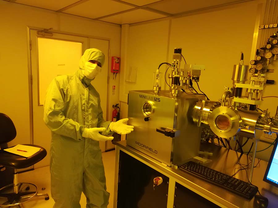
The work was carried out using a MiniLab 125 series tool equipped with actively-cooled 3” sources for 3” targets, an RF power supply, substrate heating and rotation, and a process chamber base pressure of <5 × 10⁻⁸ mbar. The tool also had a load-lock for fast sample introduction and sustained low base pressures. A pre-deposition etch cleaning module allowed for optimised surface preparation.